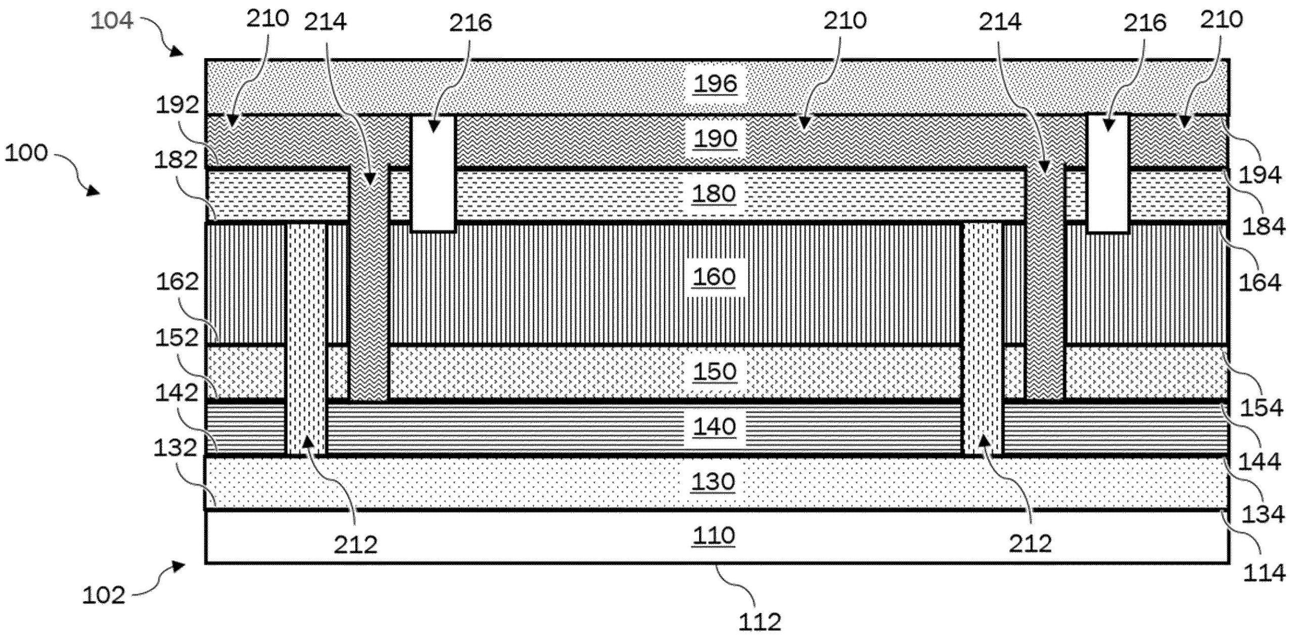
First Solar has filed a patent for a method of scribing a layer stack in a photovoltaic device. The method involves using a laser scribing waveform with specific pulse groupings and pulse widths to create a scribe through the layers. The pulse groupings repeat at a group repetition period of at least 1.5 µs, and each pulse within the groupings has a width of no more than 900 fs. GlobalData’s report on First Solar gives a 360-degree view of the company including its patenting strategy. Buy the report here.
According to GlobalData s company profile on First Solar, photovoltaic roof tiles was a key innovation area identified from patents. First Solar's grant share as of June 2023 was 1%. Grant share is based on the ratio of number of grants to total number of patents.
Method for laser scribing a photovoltaic device layer stack

A recently filed patent (Publication Number: US20230187572A1) describes a method for scribing a layer stack of a photovoltaic device using laser technology. The method involves directing a laser scribing waveform to the film side of the layer stack, creating a scribe through one or more layers of the stack. The laser scribing waveform consists of pulse groupings that repeat at a group repetition period of at least 1.5 µs. Each pulse grouping contains two or more pulses that repeat at a pulse repetition period of no more than 100 ns, with each pulse having a pulse width of no more than 900 fs.
The method also includes generating relative motion between the laser scribing waveform and the layer stack at a scan rate of at least 1 m/s. Additionally, each pulse in the waveform has a beam diameter between 0.5 µm and 20 µm, and a pulse energy of no more than 10 µJ. The wavelength of each pulse falls within the range of 300 nm to 1,100 nm, or more specifically, between 300 nm and 600 nm.
The layer stack being scribed may include various layers such as an absorber layer containing cadmium and tellurium, a TCO layer, and a back contact layer adjacent to a conductive layer. The scribe is formed without traversing any intervening layers between the absorber layer and the substrate.
The scribe created by the laser scribing waveform defines a counter that extends through the laser effected width of the scribed layers. The laser effected width is no more than 40 µm. The scribe also includes sidewalls that extend from a portion of the scribed layers adjacent to the laser effected width to a trough. The trough represents the area where at least 99% of the thickness of the scribed layers is removed. The trough width is no more than 15 µm.
The ratio of the removal width, defined by the sidewalls at a 90% thickness of the scribed layers, to the trough width is at least 5, or falls within the range of about 12 to about 25. Furthermore, the sidewalls form a maximum acute angle a with respect to the first surface of the scribed layers.
This patent application presents a method for scribing a layer stack of a photovoltaic device using laser technology. The specific parameters of the laser scribing waveform, such as pulse repetition period, pulse width, and beam diameter, along with the scan rate, ensure precise and efficient scribing. The method allows for the creation of a scribe without traversing intervening layers, providing a clean and accurate scribing process. The resulting scribe features sidewalls and a trough that remove a significant portion of the layer thickness, enhancing the performance of the photovoltaic device.
To know more about GlobalData s detailed insights on First Solar, buy the report here.
Data Insights
From

The gold standard of business intelligence.
Blending expert knowledge with cutting-edge technology, GlobalData’s unrivalled proprietary data will enable you to decode what’s happening in your market. You can make better informed decisions and gain a future-proof advantage over your competitors.


